Research
We use light to understand and control materials, develop new ways to measure the unmeasurable, and engineer the next generation of electronic and optical technologies.
We do this so that….
Semiconductor memories last longer
Defects limiting performance are identified and controlled
Stress & temperature are imaged at previously inaccessible scales
Spectroscopic tools deliver greater capability in smaller packages
We combine spectroscopy, thermal physics, nanophotonics, and materials engineering to connect fundamental physical mechanisms with device performance.
Current Research Areas
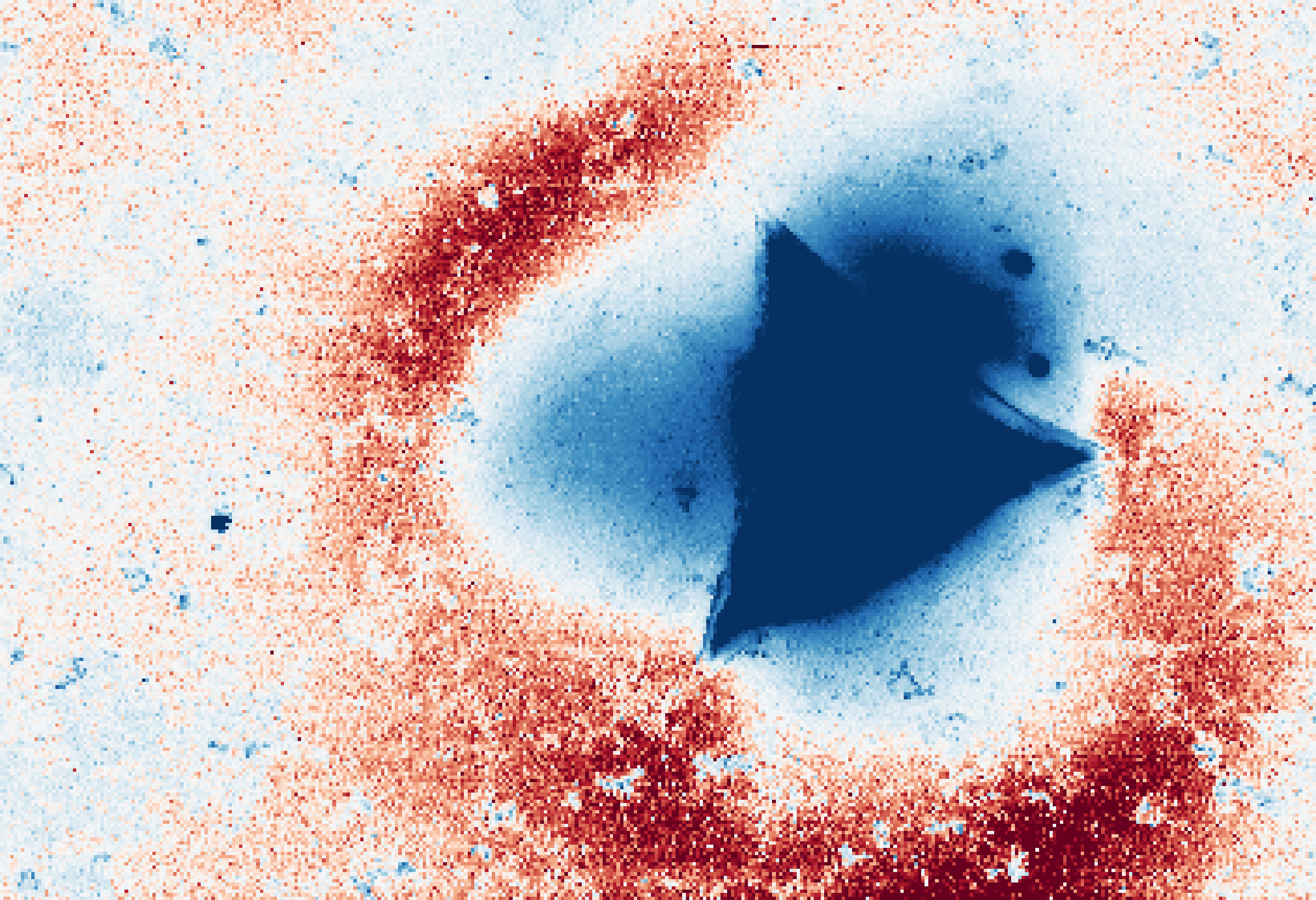
STRAIN & PROCESSING OF FERROELECTRIC OXIDES (NSF)
Problem: Ferroelectric hafnia-based oxides offer a promising path toward energy-efficient memory integrated near logic, but their performance depends strongly on processing, strain, phase, and defect structure. Conventional thermal processing can also conflict with the temperature limits of back-end-of-line (BEOL) semiconductor fabrication, creating a need for both new processing strategies and nanoscale methods to understand how these materials respond.
Path: The STEP FOx project combines localized laser annealing with device-scale characterization to develop BEOL-compatible ferroelectric oxides. Within this effort, we fabricate and electrically characterize devices following laser processing and use near-field infrared spectroscopy to probe material behavior at the nanoscale. We are also developing near-field IR methods for mapping localized stress and deformation in model oxide systems such as α-quartz, providing a foundation for future measurements of strain, phase, and defects in scaled ferroelectric devices.

Emerging Material Systems
Problem: New materials are needed for applications in computing, sensing, water-treatment, and imaging. Material development requires means to determine the links between process and properties.
Path: Advanced spectroscopic techniques like Raman, FTIR, and IR-ellipsometry provide such information. We use these techniques to help advance next-generation ferroelectrics, oxides, and 2D-materials.

near-field radiative cooling (CTRC)
Problem: Radiation is traditionally not a factor in the design of electronics cooling because its quartic relationship with temperature is typically outpaced by conduction/convection. However, electronics are getting too hot, and devices are too small to effectively shed heat with current carriers. We need to find how “small” carriers like photons can assist “big” carriers like phonons.
Path: Radiative flux can be increased orders of magnitude when two objects are brought into the near-field (within the thermal wavelength), and the evanescent fields interact with each other. Photons are now able to tunnel across the gap and add new modes of heat transfer. We seek ways of using this phenomenon to help cool next-generation electronics.
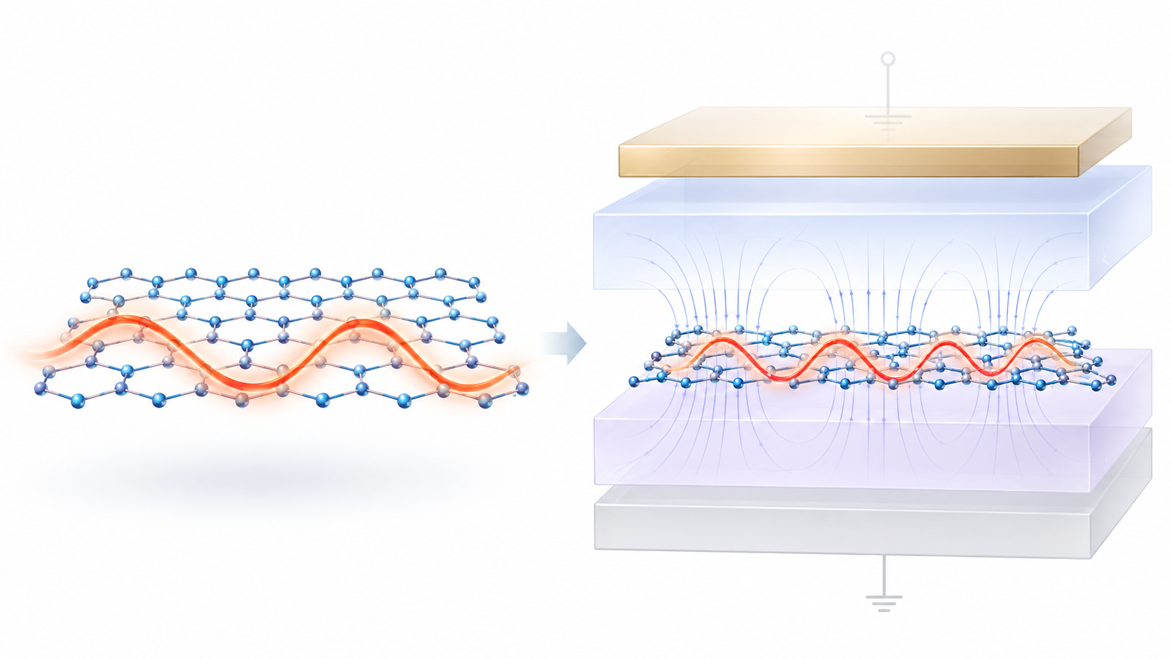
Electrostatic Effects on Phonon Properties
In Collaboration with Sustainable Energy and Nanoscale Transport Lab, PI: Xiulin Ruan
Problem: Future transistors require semiconductor channels only a few atoms thick. 2D materials can provide these channels, but their extreme thinness (large surface-to-volume ratio) also makes them highly sensitive to the materials around them. Phonons limit charge transport and dictate heat transfer through a device, yet these vibrations can change when the 2D material is placed next to substrates or gate dielectrics. Understanding these effects can provide useful guidance for integrating 2D materials into future electronic devices.
Path: Use density functional theory alongside lattice dynamics calculations to determine how the surrounding dielectric environment modifies phonons in 2D materials.
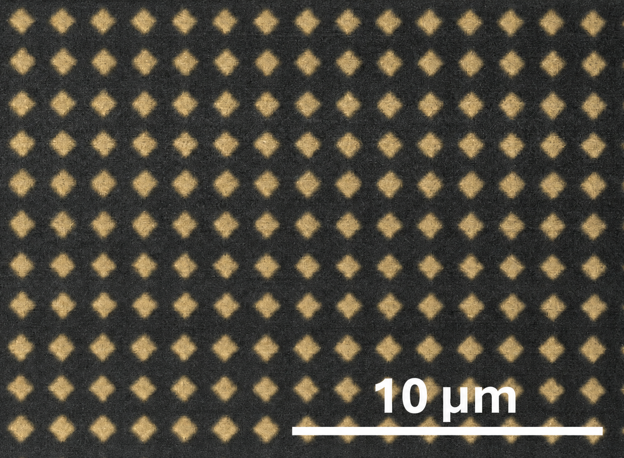
Task Specific Spectroscopy
Problem: Conventional spectrometers are bulky and general-purpose, limiting their sensitivity and practicality for targeted sensing tasks.
Path: Use machine learning to tailor metasurfaces (ultrathin optical filters made from nanoscale structures) to specific sensing applications, then combine them with compressed sensing to create compact, highly sensitive spectrometers.
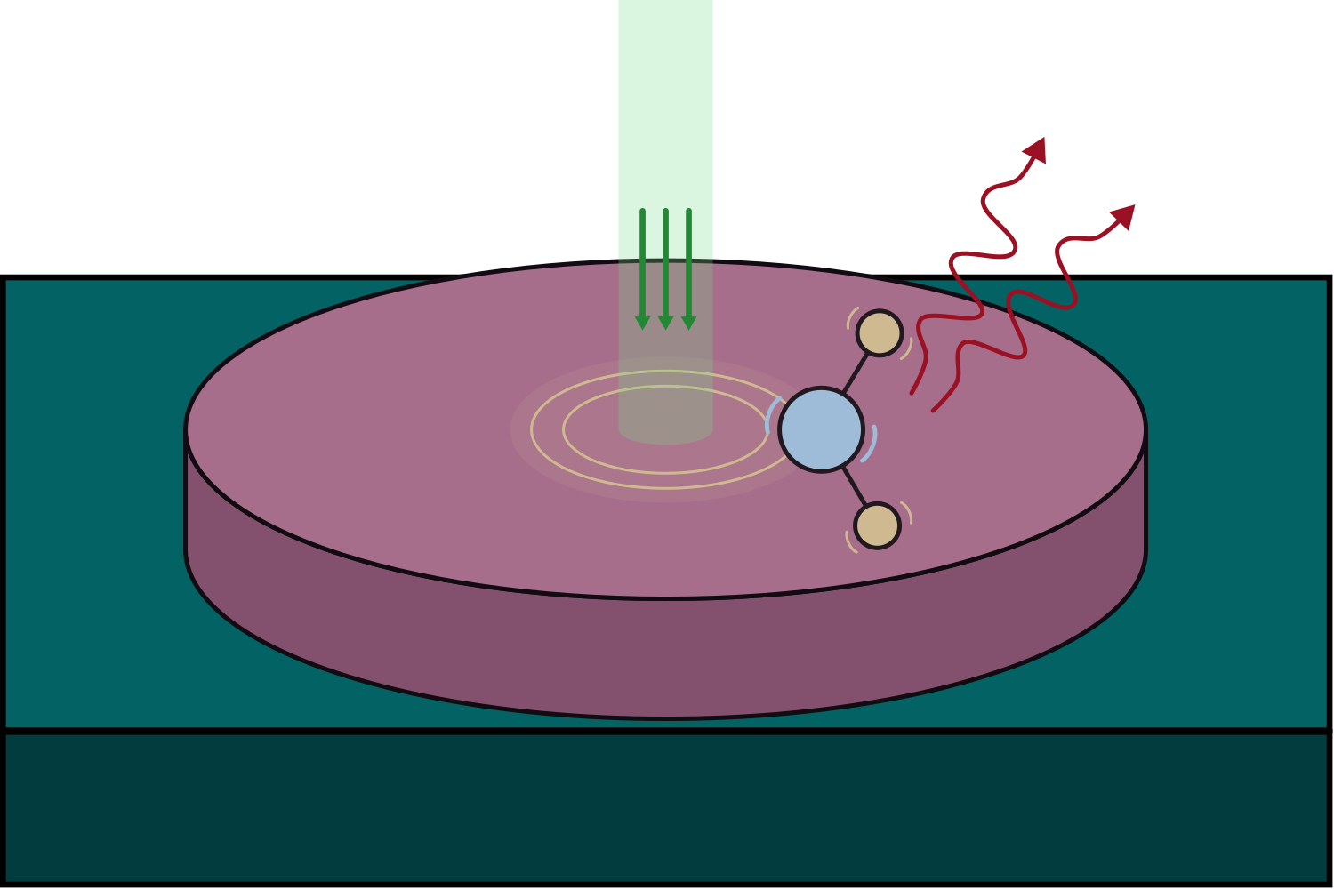
Phonons in Indirect Bandgap Lasing
Problem: Thin tungsten disulfide (WS2) discs have shown indirect bandgap lasing and could offer a path to easier integration of photonic light sources with other materials. Indirect emission requires vibrations of the crystal lattice via phonons to conserve momentum. Their role in the strong emission from these discs remains unclear.
Path: Raman spectroscopy, which probes phonons and local temperature, is combined with photoluminescence spectroscopy to relate phonon responses to the light emission from WS2 photonic sources.

mechanics of nanoscale through silicon vias (nano-tsv)
In Collaboration with Alpha Lab, PI: Tiwei Wei
Problem: More densely packed computing architectures requires more connections. Wires need to go in 3-dimensions to connect one silicon chip to another. This requires extremely small holes called to be “drilled” into the silicon and filled with metal. We call these filled holes through silicon vias. At present, these vias are too big. Making them smaller is hard because they break and can push or pull on the Si-transistors so much that the devices don’t work as well in their presence. Ways to make the vias smaller have to be created.
Path: Leverage plasticity to enable more dense packing of nano-TSV’s. Check progress by imaging strain with Raman spectroscopy.